

Construction time: November 15, 2019 - July 31, 2021
Building area: 78,000㎡,Clean area: 22,000㎡
Cleanliness level: Class 100 - 1,000
Scope of contracting: EPC construction general contracting
Project process equipment: Mask aligner
Project highlights:the design, procurement, construction, management, trial operation, acceptance and warranty services for construction engineering, structural engineering, decoration engineering, water supply and drainage engineering, elevator engineering, space management engineering, cleanroom engineering, ventilation and air conditioning engineering, power engineering, power supply and lightning protection engineering, anti-static engineering, electric power engineering, lighting engineering, communication engineering, automatic control engineering, weak power engineering, professional system engineering, external works, secondary distribution system engineering of production process equipment (excluding machine handling, installation and equipment internal connection), and three supplies and one leveling within the boundary line of the preliminary design land.

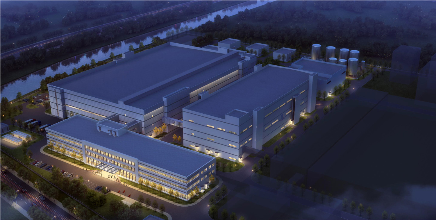
Aerial view