

Construction time: April 30, 2020 - September 12, 2020
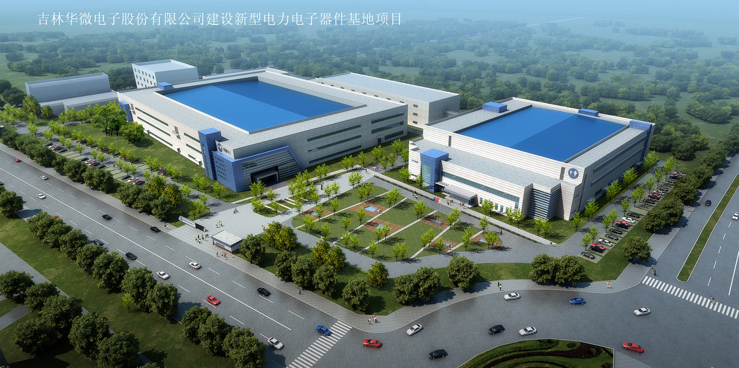
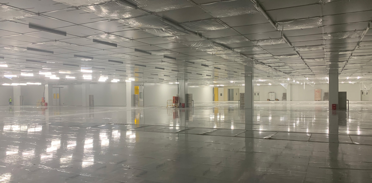
Building area: 47,517.75㎡, Clean area: 8,800㎡
Cleanliness level: Maximum Class 100
Scope of contracting: Jilin Sino-Microelectronics chip plant clean pack
Project highlights:this project is about the procurement and supply, transportation (including secondary lightering), unstuffing and unloading, warehousing, placement, installation and commissioning, trial operation, cooperative acceptance, after-sales service, quality guarantee period, and other related services of the corresponding cleanrooms and general electromechanical systems. These systems include but are not limited to: cleanroom environment system, cleanroom fresh air treatment system, process exhaust system, electrical system, automatic control system, water supply and drainage system, comprehensive wiring system, fire alarm system, VESDA system, smoke control and extraction and emergency exhaust system, and construction and decoration system.
Industry value:Sino-Microelectronics has several production lines of 3-inch, 4-inch, 5-inch and 6-inch power semiconductor discrete devices and IC chips, with the chip processing capacity of more than 3 million pieces per year, and the packaging capacity of 3 billion pieces per year. Sino-Microelectronics has become one of the largest semiconductor power device manufacturing bases in China.

Aerial view of the project
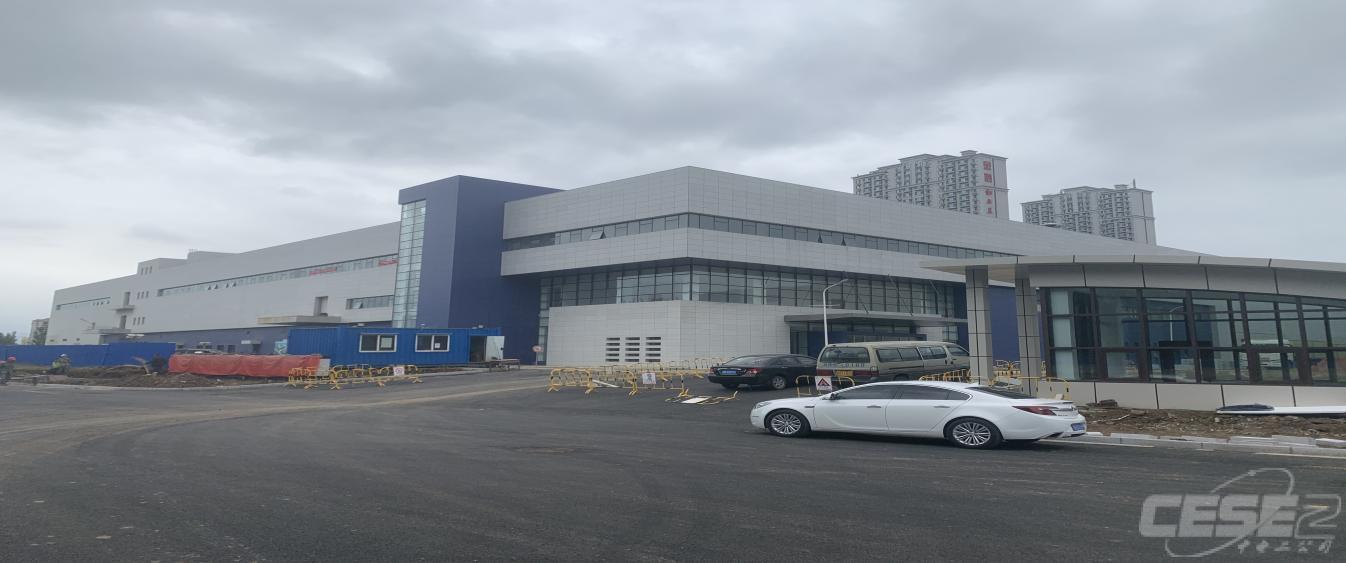
Real shots of exterior view