


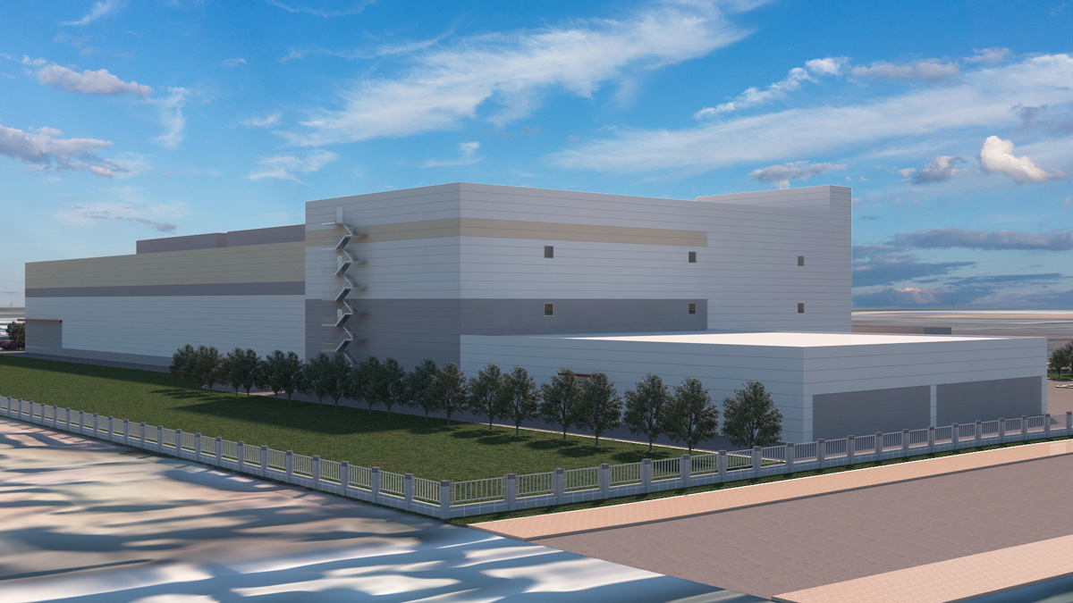
Construction time: July 1, 2020 - July 1, 2021
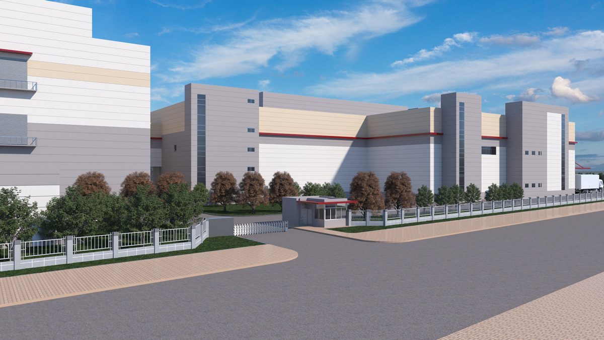
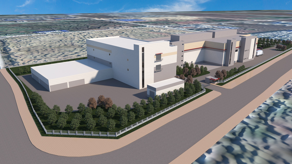
Building area: 27,776㎡,Clean area: 3,076㎡
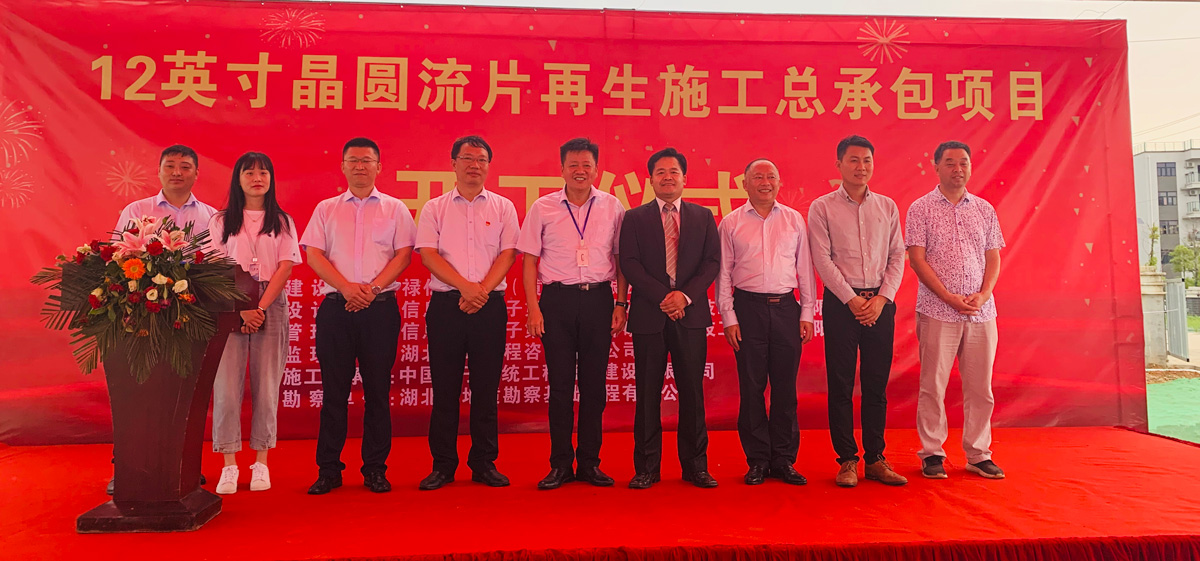
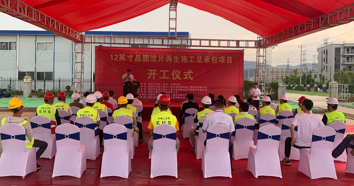
Scope of contracting: general contracting of Luyi Semiconductor civil construction and general contracting of Luyi Semiconductor electromechanical engineering
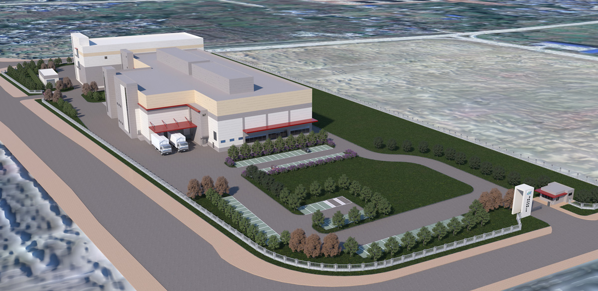
Project highlights: Luyi Semiconductor (Huangshi) Co., Ltd. 12-inch Wafer Tape-out Regeneration Project is located in Tieshan Area, Huangshi Economic & Technological Development Area, and is mainly engaged in the regeneration services. The test wafers and blocking wafers used in wafer manufacturing are sorted, cleaned, ground, polished, purified and dried to the same level of cleanliness and flatness as the new test wafers after the process is completed, and then provided again for use as blocking/controlling wafers. The air cleanliness level in some areas of the cleanroom for processing wafers reaches the ISO Class 1, that is to say, particles with a particle size of less than 0.1μm are less than 10 particles/m³ in the air.
Industry value:after the full completion of the project, it can achieve a monthly production capacity of 400,000 wafers, which will provide test wafers, blocking wafers and other wafer regeneration services for large-scale integrated circuit enterprises in the country.
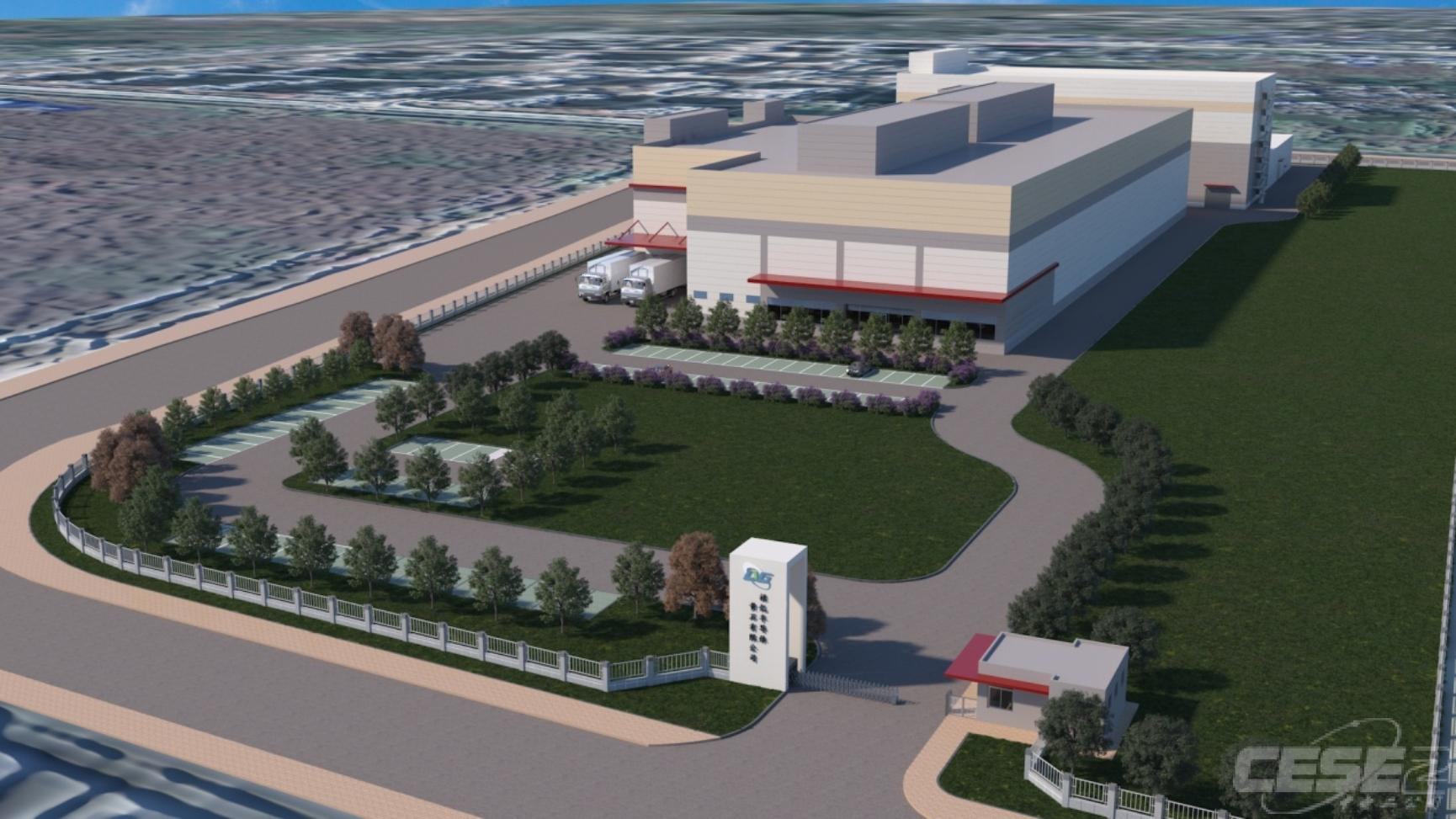
Aerial view
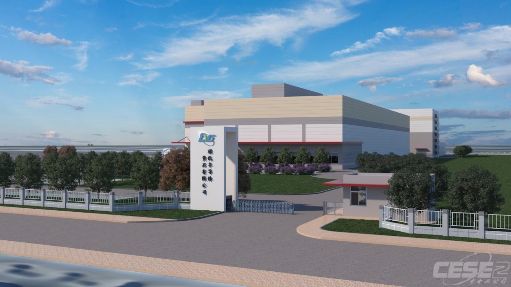
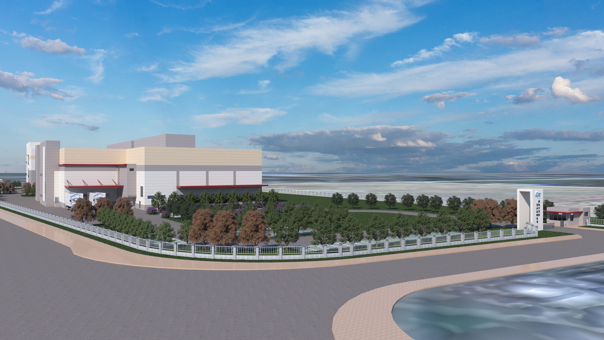
Aerial view